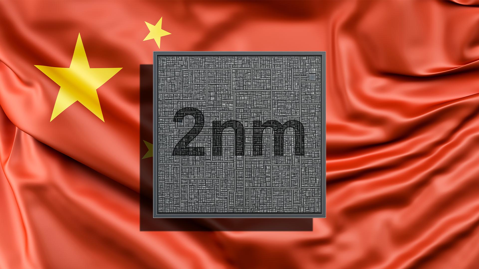

The path to profitability for Samsung’s foundry enterprise implies that it must safe a plethora of shoppers for its 2nm GAA course of. To this point, the Exynos 2600 is recorded to be the primary SoC to be mass produced on this lithography, with Tesla additionally having secured a multi-billion-dollar deal with the Korean giant. Now, the newest report states that two Chinese purchasers have lined as much as place 2nm GAA orders for his or her upcoming cryptocurrency mining merchandise, suggesting that Samsung is slowly progressing in the fitting route. Nonetheless, it’s removed from a place the place it can provide TSMC a run for its cash.
The highest Chinese cryptocurrency mining gear producer, Bitmain, is presently not bought on the concept of utilizing Samsung’s 2nm GAA chips, and is sticking with TSMC
The 2 Chinese cryptocurrency mining gear producers, based on Korean media outlet Hankyung, are MicroBT and Canaan. Each clients will reportedly use Samsung’s 2nm GAA chips because the ‘brains’ of their upcoming cryptocurrency mining {hardware}. MicroBT and Canaan are presently the world’s second and third largest producers of this particular paraphernalia, with Bitmain being the biggest entity on this area.
Nonetheless, BITMAIN has but to position any orders with Samsung, with the report stating that the corporate is sticking with TSMC, seemingly as a result of receiving well timed orders, accessing cutting-edge expertise, and its skill to beat poor yields, which is an impediment that Samsung has but to show with its 2nm GAA node.
The chip maker has already commenced manufacturing of MicroBT’s orders, with Canaan planning to place its first silicon into manufacturing in early 2026. Deliveries are anticipated to occur within the second half of subsequent yr. Each cryptocurrency mining corporations’ orders will enter manufacturing at Samsung’s S3 line in Hwaseong, Gyeonggi Province.
These orders equate to round 10 p.c of the corporate’s complete 2nm manufacturing capability, with round 2,000 month-to-month 300mm (12-inch) sheets getting produced. Although the amount isn’t important, it’s proof that Samsung needs to be on equal footing with TSMC and is aiming to safe as many purchasers as attainable for the bleeding-edge lithography.
Earlier, we reported that Snapdragon 8 Elite Gen 5 samples on the 2nm course of have been sent to Qualcomm for evaluation purposes, however a dual-sourcing method that features Samsung may solely occur with the Snapdragon 8 Elite Gen 6 launching in late 2026. To hold tempo with TSMC, Samsung was earlier reported to have completed the basic design of its second-generation 2nm GAA process, and can also be developing the third iteration, often known as SF2P+.
The 2nm GAA expertise may even witness a manufacturing plan at Samsung’s Taylor plant situated in Texas. Solely just lately, ASML was reported to type a workforce that might be responsible for the delivery and installation of necessary equipment to begin next-generation wafer manufacturing. With this step accomplished, the U.S. facility is able to producing greater than 15,000 wafers monthly via 2027.
Information Supply: Hankyung
Comply with Wccftech on Google to get extra of our information protection in your feeds.


